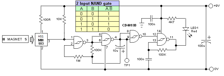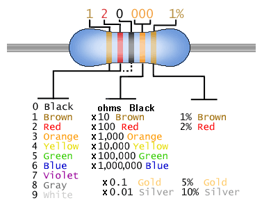


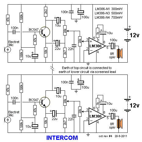
This circuit uses a single
transistor and LM386 amplifier IC to produce an intercom that
allows hands-free operation.
As both microphones and loudspeakers are always connected, the
circuit is designed to avoid feedback - known as the "Larsen
effect".
The microphone amplifier transistor is 180° phase-shifted and
one of the audio outputs is taken at the collector and its
in-phase output taken at the emitter. These are mixed by the
10u, 22u, 20k pot and 2k7 so that the two signals almost cancel
out. In this way, the loudspeaker will reproduce a very faint
copy of the signals picked-up by the microphone.
At the same time, as both collectors of the two intercom units
are tied together, the 180° phase-shifted signal will pass to
the audio amplifier of the second unit without attenuation, so
it will be loudly reproduced by its loudspeaker.
The same operation will occur when speaking into the microphone
of the second unit. When the 20k pot is set correctly, almost no
output will be heard from the loudspeaker but a loud and clear
reproduction will be heard at the output of the other unit.
The second 20k pot adjusts the volume.
This is the third part of our Circuits e-book series.
It contains a further 100 circuits.
This time we have concentrated on circuits containing one or more IC's.
It's amazing what you can do with transistors but when Integrated Circuits came along, the whole field of electronics exploded.
IC's can handle both analogue as well as digital signals but before their arrival, nearly all circuits were analogue or very simple "digital" switching circuits.
Let's explain what we mean.
The word analogue is a waveform or signal that is changing (increasing and decreasing) at a constant or non constant rate. Examples are voice, music, tones, sounds and frequencies. Equipment such as radios, TV's and amplifiers process analogue signals.
Then digital came along.
Digital is similar to a switch turning something on and off.
The advantage of digital is two-fold.
Firstly it is a very reliable and accurate way to send a signal. The signal is either HIGH or LOW (ON or OFF). It cannot be half-on or one quarter-off.
And secondly, a circuit that is ON, consumes the least amount of energy in the controlling device. In other words, a transistor that is fully turned ON and driving a motor, dissipates the least amount of heat. If it is slightly turned ON or nearly fully turned ON, it gets very hot.
And obviously a transistor that is not turned on at all will consume no energy.
A transistor that turns ON fully and OFF fully is called a SWITCH.
When two transistors are cross-coupled in the form of a flip flop, any pulses entering the circuit cause it to flip and flop and the output goes HIGH on every second pulse. This means the circuit halves the input pulses and is the basis of counting or dividing. It is also the basis of a "Memory Cell" as will will hold a piece of information.
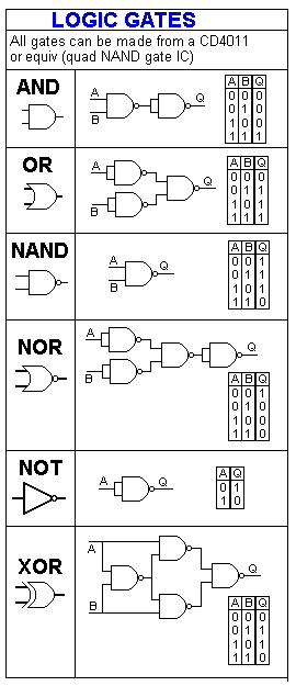
Digital circuits also introduce the concept of two inputs creating a HIGH output when both are HIGH and variations of this.
This is called "logic" and introduces terms such as "Boolean algebra" (Boolean logic) and "gates."
Integrated Circuits started with a few transistors in each "chip" and increased to mini or micro computers in a single chip. These chips are called Microcontrollers and a single chip with a few surrounding components can be programmed to play games, monitor heart-rate and do all sorts of amazing things. Because they can process information at high speed, the end result can appear to have intelligence and this is where we are heading: AI (Artificial Intelligence).
In this IC Circuits ebook , we have presented about 100 interesting circuits using Integrated Circuits.
In most cases the IC will contain 10 - 100 transistors, cost less than the individual components and take up much less board-space. They also save a lot of circuit designing and quite often consume less current than discrete components or the components they replace.
In all, they are a fantastic way to get something working with the least componentry.
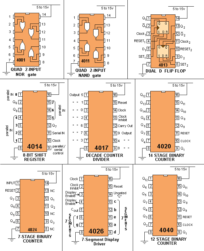
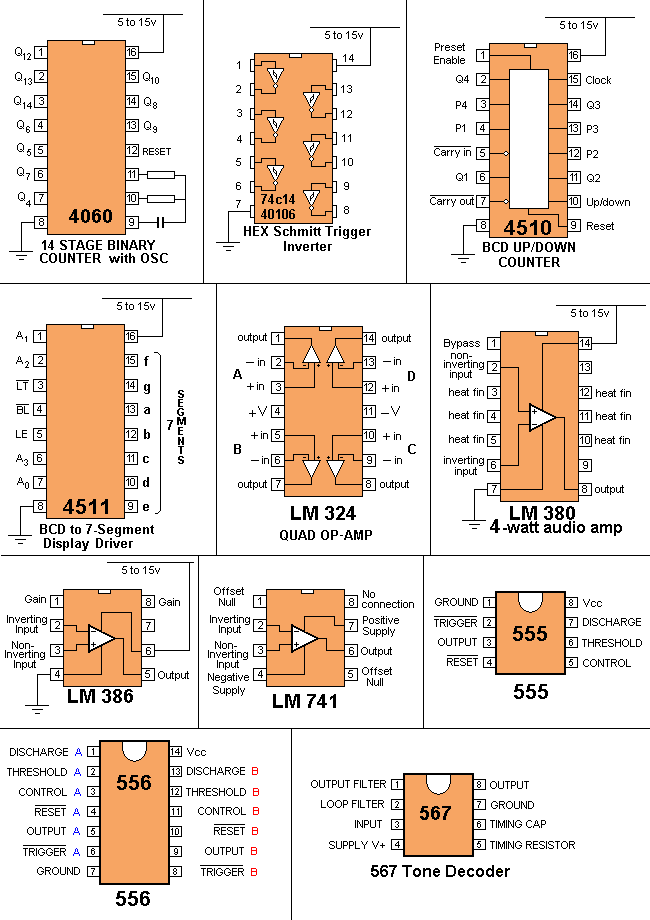
A list of of some of the most common Integrated Circuits (Chips) is provided at the end of this book to help you identify the pins and show you what is inside the chip.
Some of the circuits are available from Talking Electronics as a kit, but others will have to be purchased as individual components from your local electronics store. Electronics is such an enormous field that we cannot provide kits for everything. But if you have a query about one of the circuits, you can contact me.
Colin Mitchell
TALKING ELECTRONICS.
talking@tpg.com.au
To save space we have not provided lengthy explanations of how the circuits work. This has already been covered in TALKING ELECTRONICS Basic Electronics Course, and can be obtained on a CD for $10.00 (posted to anywhere in the world) See Talking Electronics website for more details: http://www.talkingelectronics.com
MORE INTRO
We have said this before abut we will say it again:
There are two ways to learn electronics.
One is to go to school and study theory for 4 years and come out with
all the theoretical knowledge in the world but very little practical
experience. The other is to "learn on the job."
I am not saying one approach is better than the other but most electronics
enthusiasts are not "book worms" and many have been dissuaded
from entering electronics due to the complex mathematics surrounding
University-type courses.
Our method is to get around this by advocating designing, building,
constructions and even more assembly with lots of experimenting and when
you get stuck with a mathematical problem, get some advice or read about
it via the thousands of free test books on the web.
Anyone can succeed in this field by
applying themselves to constructing
projects. You actually learn 10 times faster by doing it yourself and we
have had lots of examples of designs from students in the early stages
of their career.
And don't think the experts get it right the first time. Look at all the
recalled electronics equipment from the early days.
The most amazing inventions have come from almost "newcomers" as
evidenced by looking through the "New Inventions" website.
All you have to do is see a path for your ideas and have a goal that you
can add your ideas to the "Word of Invention" and you succeed.
Nothing succeeds like success. And if you have a flair for designing
things, electronics will provide you a comfortable living for the rest of your
life.
The market is very narrow
but new designs are coming along all the time and new devices
are constantly being invented and more are always needed.
Once you get past this eBook of "Chips" you will want to
investigate microcontrollers and this is when your options will explode.
You will be able to carry out tasks you never thought possible, with a
chip as small as 8 pins and a few hundred lines of code.
In two weeks you can start to understand the programming code for a
microcontroller and perform simple tasks such as flashing a LED and
produce sounds and outputs via the press of a button.
All these things are covered on
Talking Electronics website
and you don't have to buy any books or publications. Everything is
available on the web and it is instantly accessible. That's the beauty
of the web.
Don't think things are greener on the other side of the fence, by buying
a text book. They aren't. Everything you need is on the web AT NO COST.
The only thing you have to do is build things. If you have any
technical problem at all, simply email
Colin Mitchell
and any question will be answered. Nothing could be
simpler and this way we guarantee you SUCCESS. Hundreds of readers have
already emailed and after 5 or more emails, their circuit works. That's
the way we work. One thing at a time and eventually the fault is found.
If you think a circuit will work the first time it is turned on, you are
fooling yourself.
All circuits need corrections and improvements and that's what makes a
good electronics person.Don't give up. How do you think all
the circuits in these eBooks were designed?
Some were copied and some were designed from scratch but all had to be
built and adjusted slightly to make sure they worked perfectly.
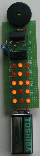
I don't care if you use bread-board, copper strips, matrix board or
solder the components in the air as a "bird's nest." You only learn when the
circuit gets turned on and WORKS!
In fact the rougher you build something, the more you will guarantee it will
work when built on a printed circuit board.
However, high-frequency circuits (such as 100MHz FM Bugs) do not
like open layouts and you have to keep the construction as tight as
possible to get them to operate reliably.
In most other cases, the layout is not critical.
If you just follow these ideas, you will succeed.
A few of the basics are also provided in this eBook, the first is
transistor outlines:
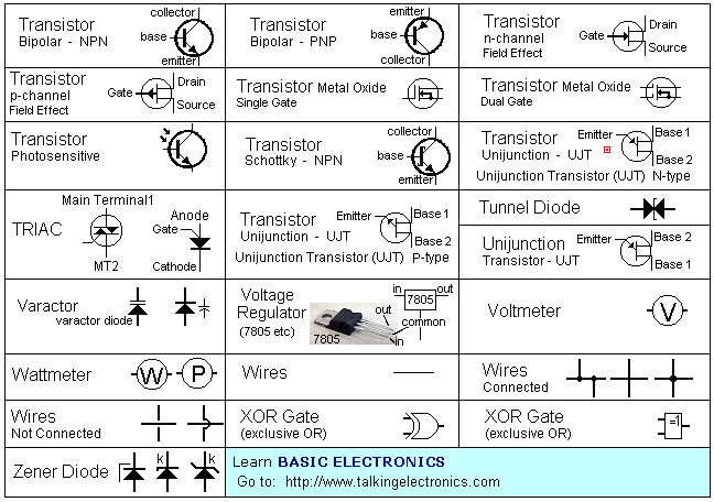
TRANSISTORS
Most of the transistors
used in our circuits are BC 547 and BC 557. These are classified as
"universal" or "common" NPN and PNP types with a voltage rating of about
25v, 100mA collector current and a gain of about 100.
You can use almost any type of transistor to replace them and here is a list of
the equivalents and pinouts: